Overview
This page will cover the full testing procedure expected of sites receiving the travelling module. The procedure consists of:
- Reception inspection
- Basic communication
- Trim IREF, VREF and voltage regulators
- Scans (including pre-tune scans, tuning, and post-tuning scans) & plotting
Here is a checklist to keep track of all the tasks. We suggest printing it out to tick off items whilst testing.
Reception inspection
These basic tasks should be performed upon receiving the package:
- Please note in the table, here when the module was recieved.
- Please take photos of the package, as well as performing a visual inspection of the module, being careful to note down (and photograph) any scratches or damage on the board. In addition, please check the wire bond connections under a microscope to make sure there is no detachment during transport.
- Check that the jumpers on the Single Chip Card (SCC) are correct. Complete SCC configuration is listed here (Note that
PLL_RSTjumper is missing on the diagrams, which however should be there as mentioned in the recommended configuration.) In particular, note:- The pin headers labelled
PWR_AandPWR_D(outlined in red box in image) should both be set toVINAandVIND, respectively. This is done by setting the jumper to connect the left and middle pin for each set of three pins (when the board is orientated as seen in the photo). Setting these jumpers ensures the voltage regulators are used during operation. Setting these incorrectly could lead to permanent damage in the chip. - Check that the PLL and CML drivers are being powered from VDDA by setting VDD_PLL_SEL and VDD_CML_SEL to VDDA, respectively (left most pins for each set of 6 in yellow box in photo).
- Make sure, for normal operation, that both the
VREF_ADCandIREF_IOpin headers both have jumpers on them. - Ensure that there are jumpers solder to pads
JP10andJP11. -
Finally, ensure that there is a jumper across the
PLL_RSTpin header.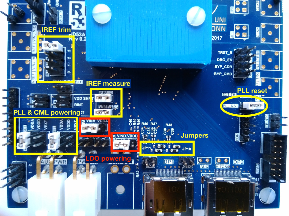
- The pin headers labelled
Basic communication
With the chip inspected and jumpers set correctly on the SCC, make a quick check of your scanning setup by configuring the chip.
- Remember! Tests should be done at room temperature with the chip powered in LDO mode at 1.8V. If using direct powering (not recommended) DO NOT exceed 1.3V, anything higher will likely to result in permanent damage.
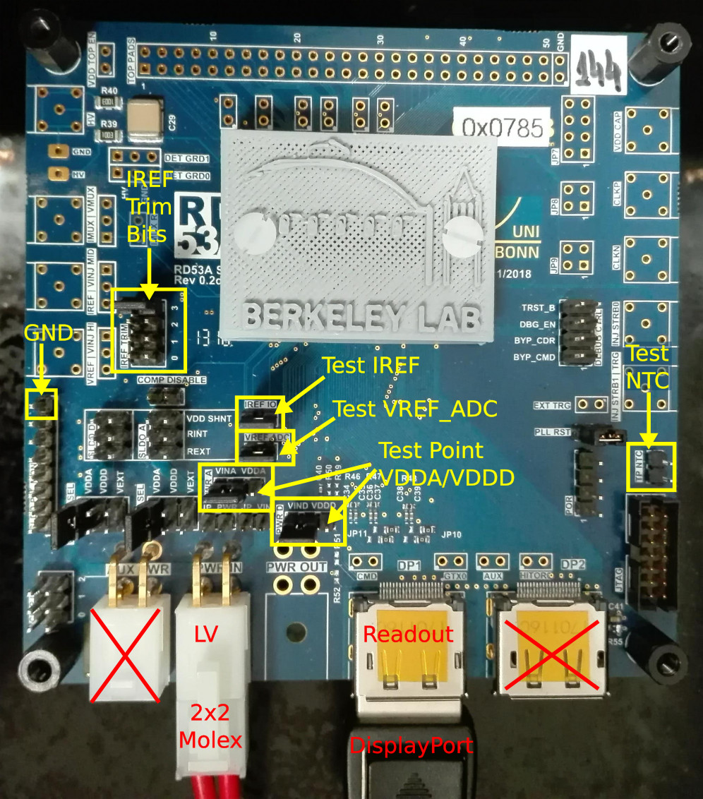
Connect the Low Voltage (LV) supply via Molex to the PWR_IN connector, as shown in the photo below. If you are unclear as to how to set up your LV supply, please see the instructions in Experimental setup. Connect the SCC to your readout system (be it YARR or BDAQ) using a displayport connector, as seen in the photo below.
Next, edit the configuration (config) file used for these tests. BDAQ and YARR use different default configs:
- YARR uses: rd53a_TravellingChip.json
- BDAQ uses: rd53a_TravellingChip.cfg.yaml
NB: To enable an easier comparison between the two systems these configs differ from the default configs found in both systems according to these guidelines (5uA/pixel inner layer).
Tasks:
- Please change the chip name in the config to the serial number of your chip (e.g. 0x495 for travelling module 3). The chip name in each config file is:
"Name":in YARRchip_sn:in BDAQ
- Run a digital scan and check the output - this is just to see if you can communicate with the chip and to test your basic setup. If you have any chip communication problems it may be that the internal voltages supplied from the LDO is not adequate, which will be fixed in the next step.
Trim IREF, VREF_ADC and the voltage regulators
In this step you will trim the reference current and supplied internal voltages by (a) measuring either a current or voltage and (b) modifing the jumpers on the board or parameters in the configuration file.
IREF trim
- CAUTION: Injecting current into the IREF instead of measuring it could permanently damage the chip. DO NOT attempt to measure the current across IREF if you are unsure how to!!
Tasks:
- Power down the LV supply.
- On the SCC, remove the jumper across the pin header labeled
IREF_IO(see photo). - Set up a current measuring device such as the Keithley 2400 and set it up to measure a current. Please do not use a simple multimeter for this task as it is usually not accurate enough. Ensure that the range of the device is set to measure at least 4 μA, on the Keithley this is achieved by setting the measurement display range to at least 10 μA.
- Connect the current-measuring device to the
IREF_IOpin headers. - Power up the LV supply as before and measure the current.
- If the current is NOT 4.0 μA you can trim it using the
IRE_TRIMbits on the SCC. This is a 4-bit register, so you can use multiple jumpers to trim. - Make note of the final jumper configuration on
IREF_TRIMand the current measurement. - Power down the LV supply, disconnect the connectors to
IREF_IO, and replace the jumper acrossIREF_IO.
VREF_ADC trim
Measure the jumper with the label VREF_ADC against GND. Adjust the DACs so that this value is as close to 0.9 V as possible. This step is essential for the threshold tunings to be correct.
- YARR:
AdcRefTrim - BDAQ:
MON_BG_TRIM
Internal voltage (VDD) trimming
If you previously were not able to configure the chip, it may be because the internal voltages supplied from the regulators were too low. This step will measure these voltages and show you how to correct them.
Tasks:
- Power up the chip and configure it with the same config file you used previously.
- Using a voltmeter, probe VDDA/D with respect to ground. You can find the VDDA/D test pin on the third pin of
PRW_A/Das pointed out on the picture. There are multiple ground references on the board, such as the top-most pin of theSLDO_PLL_MONarray or any Lemo case. - If the voltage is not 1.2 V, edit the respective trim in the chip config file:
- YARR:
SldoAnalogTrimfor VDDA andSldoDigitalTrimfor VDDD. - BDAQ:
VREF_A_TRIMfor VDDA andVREF_D_TRIMfor VDDD.
- YARR:
- Re-configure the chip and repeat steps (2) and (3) until VDDA is as close to 1.2 V as possible.
- If communication issues still persist, e.g.
data not validin YARR, try to increase or decrease VDDA slightly until these disappear. - Record both the voltages measured and the final trim values used.
If, however, after trimming the voltages you are still unable to communicate with the chip having tried these measures, please see FAQ & Troubleshooting.
Scanning and tuning
After the IREF and voltage references have been trimmed accordingly, we are ready to run some scans. But first:
- Power-cycle the chip and record the current drawn when the LV supply is powered, before the chip is configured.
- Record the current drawn by the chip on the LV supply after the chip is configured.
For the travelling module, we require that all three FE variants (synchronous, linear and differential) on RD53A module are tuned. Whilst running these scans, the temperature of the chip should be monitored via the TP_NTC pin header (see experimental setup for details). This temperature log, as well as the output of the scans listed below, should all be saved to the database.
The general scan procedure is as follows:
-
Pre-tuning scans should be run over all frontends:
- Digital scan
- Analog scan
- Threshold scan
-
Tunings should be performed on each frontend separately. The threshold of all three FE can be tuned to 1000e. For the linear frontend the tuning has to start with 2000e and retuned to 1000e for both global and pixel threshold tunings. The ToT should be tuned to 8BC at 10000e:
- Global threshold tuning
- Pixel threshold tuning (not for syncFE)
- Time over threshold tuning
- Re-adjust pixel threshold (not for syncFE)
-
Post-tuning scans should be run over all frontends:
- Threshold scan
- ToT scan
- Noise scan
-
Post processing (YARR ONLY): plot threshold and noise distributions with ROOT scripts.
Either YARR or BDAQ can be used to run these scans. The rest of this page describes how to do this with both systems. When running threshold scan, make sure the range of injected charge covers the expected threshold. The conversion is approximately 1 DAC = 10 electrons.
- YARR:
InjVcalDiff - BDAQ: the difference between
VCAL_MEDandVCAL_HIGH
Testing with YARR
Use the scanConsole for all tunings and scans following this tuning routine.
Run each scan and tuning by hand, observe the output in the terminal and look at the plots after scanConsole is finished. Look into the chip configuration and make sure the threshold DAC for each frontend makes sense.
For pixel tuning, make sure to run FE_tune_finepixelthreshold.json after FE_retune_pixelthreshold.json for each frontend.
Before running the noise scan, please look into the pixel configuration section in the chip configuration file and make sure that not all pixels are disabled. If they are, simply run another digital scan with -m 1 to reset the enable mask followed by a normal analog scan.
Please use the ROOT scripts (Threshold and NoiseMap) to produce fitted plots which show separate the data for each FE in png format and only the good pixels in differential frontend.
Testing with BDAQ
Follow instructions
here.
You can either execute with e.g. bdaq53 scan_digital or
python scan_digital.py.
Once made sure that the module works, tune all FEs
and save the results before and after tuning. For FE specific scans and
tunings, adjust 'start_column' and 'stop_column' in the scan code
accordingly.
Pay attention to the scanning range and adjust VCAL_HIGH_start and
VCAL_HIGH_stop in the local_configuration section of the scan code
accordingly.
Start with a clean data folder, make sure you don't have old mask files in your folder. The same mask file is going to be written and rewritten for each FE step.
Pixel threshold tuning uses meta_tune_local_threshold.py.
Complete detailed instructions can be found here.